
What Is a PCB? Understanding the Backbone of Modern Electronics
- Kalyan Bhattacharjee

- Dec 22, 2025
- 4 min read

Introduction | What is a PCB & It's Applications
If you’ve ever opened up a smartphone, laptop, TV, or even a simple remote control, you’ve seen one - a flat board filled with tiny components and copper lines running like a miniature road network. That board is a PCB, and without it, modern electronics simply wouldn’t exist.
Despite being everywhere, PCBs are often misunderstood.
Many people think of them as “just a board,” but in reality, a Printed Circuit Board is the structural, electrical, and thermal foundation of almost every electronic device we use today.
Let’s break it down properly - without jargon, without fluff.
What Is a PCB (Printed Circuit Board)?
A PCB (Printed Circuit Board) is a rigid or flexible board used to mechanically support and electrically connect electronic components using conductive copper pathways etched onto its surface.
Instead of loose wires connecting components (as in early electronics), PCBs provide:
Fixed, repeatable connections
Compact design
Higher reliability
Easier mass production
In simple terms:👉 A PCB turns a circuit diagram into a real, working physical system.
Why PCBs Are So Important in Electronics
Before PCBs existed, circuits were built using point-to-point wiring. That approach worked - but it was bulky, error-prone, hard to repair, and impossible to scale. PCBs solved all of that.
Key Reasons PCBs Matter
They reduce size and weight of devices
They improve signal integrity and performance
They minimize human wiring errors
They allow automated manufacturing
They increase durability and lifespan
Here’s a lesser-known insight: Modern high-speed electronics (like 5G devices and GPUs) would be impossible without precisely engineered PCB trace layouts. Even millimeter-level mistakes can break performance.
Basic Structure of a PCB
Although designs vary widely, most PCBs share the same core layers:
Substrate (Base Material)
This is the foundation of the PCB.The most common material is FR-4 (fiberglass reinforced epoxy).
Its job:
Provide mechanical strength
Electrically insulate components
Copper Layer
Thin copper sheets are laminated onto the board and etched to form traces (the electrical pathways).
Fun fact: The width and thickness of copper traces directly affect heat dissipation and current handling - something designers carefully calculate.
Solder Mask
The colored layer (usually green) that protects copper traces.
It:
Prevents short circuits
Protects copper from oxidation
Makes soldering cleaner
The color is cosmetic green just happens to offer the best contrast during inspection.
Silkscreen
This is where you see labels, component names, logos, and markings.
It helps:
Assembly technicians
Repair engineers
Quality inspectors
Types of PCBs You Should Know About
This section covers the most common PCB types, helping you understand their structure, use cases, and advantages in modern electronics.
Single-Sided PCB
Components on one side only. Used in simple devices like calculators and power supplies. They are cost-effective and easy to manufacture, making them ideal for basic circuits.
Double-Sided PCB
Components on both sides. More compact and common in consumer electronics. This design allows higher component density and more complex circuit layouts. It also reduces the overall board size while improving signal routing efficiency.
Multilayer PCB
Contains multiple copper layers stacked together.
Used in:
Smartphones
Motherboards
Routers
GPUs
Modern CPUs often connect to 8–16 layer PCBs, sometimes more.
Flexible PCB (Flex PCB)
Made from flexible plastic substrates.
Used in:
Cameras
Wearables
Foldable phones
These allow bending without breaking electrical connections.
Rigid-Flex PCB
A combination of rigid and flexible sections. Highly reliable but expensive often used in aerospace and medical devices. This hybrid design improves durability, saves space, and reduces the need for connectors or cables.
How a PCB Is Made (Simplified)
PCB manufacturing is a precision process:
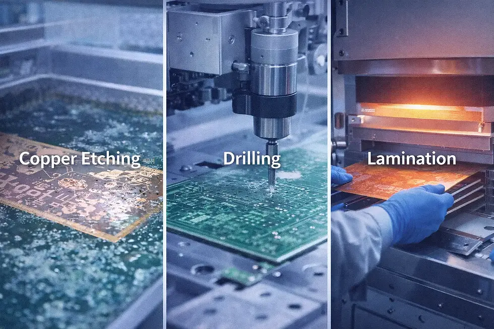
Circuit design using CAD software
Copper-clad board preparation
Photoresist application and UV exposure
Chemical etching of copper traces
Drilling holes for components
Layer lamination (for multilayer boards)
Solder mask and silkscreen application
Electrical testing and inspection
Here’s something many people don’t know: Even microscopic dust particles can ruin a PCB layer - which is why high-end PCB fabrication happens in controlled environments.
PCB vs Breadboard vs Wiring
Breadboards are for testing. PCBs are for real-world deployment.
Feature | PCB | Breadboard | Manual Wiring |
Reliability | High | Low | Medium |
Reusability | Fixed | Temporary | Limited |
Scalability | Excellent | Poor | Poor |
Manufacturing | Ideal | Not suitable | Not suitable |
Common PCB Design Challenges
Even experienced engineers face issues like:
Signal interference (EMI)
Crosstalk between traces
Heat buildup
Power distribution noise
This is why PCB design is considered a specialized engineering skill, not just “drawing lines.”
Real-World Applications of PCBs
PCBs power almost everything:
Smartphones and laptops
Medical equipment
Automotive ECUs
Industrial automation systems
Satellites and space equipment
A lesser-known fact: Modern electric vehicles contain thousands of PCBs controlling everything from battery management to braking systems.

Why PCBs Are the Unsung Heroes of Technology
PCBs don’t get the spotlight - processors, displays, and cameras do. But without PCBs, none of those components could work together reliably.
A well-designed PCB means:
Better performance
Lower failure rates
Longer product life
Easier upgrades and repairs
In short, PCBs are the silent backbone of modern electronics, turning ideas into functional, scalable, real-world devices.
Related Keywords: what is a pcb, what is a pcb board, what is a pcb circuit board, what is pcb, define pcb, pcb circuit, manufacturing printed circuit, pcb design, pcb full form, printed circuit board, types of PCB, pcb structure, pcb manufacturing process, multilayer PCB, basic structure of a pcb, types of pcb's you should know, how a pcb Is made, PCB vs Breadboard vs Manual Wiring, common pcb design challenges, real-world applications of pcb's, fintech shield


Comments